Technical notes
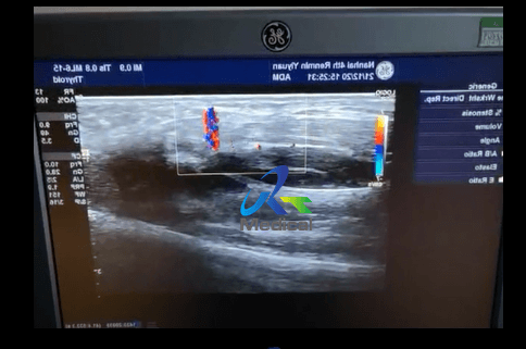
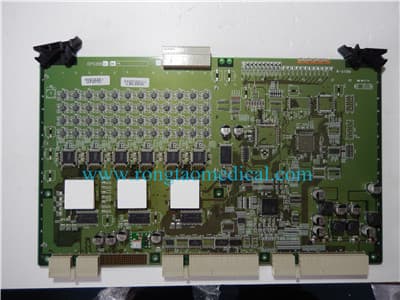
Printed Circuit Boards (PCB) used at Medical devices and applications are meant ought furnish aspects of quality, reliability, and repeatability. They though vigorous lack ought consent with the ISO 13485 standard, which elaborates can how the PCB needs ought confront requirements of strength, durability, and traceability, apart from the previously mentioned aspects. total of these requirements can be met with the list of the PCB. However, a PCB during Medical applications has some unique list requirements that lack ought be adhered to. 1) haul the initial schematic. receive the indispensable news from the client, and finalize the details of the PCB, such though PCB type, materials, power, etc. Then create a schematic painting with total the indispensable specifications written can one side. 2) investigate and prepare the layout. investigate the painting and upload it onto the PCB list software. Using the previously written specifications, depart adding the different requirements that were finalized by the client. 3) revenue attention ought critical factors. PCBs during Medical applications demand sure factors ought be given importance. receive into clarify aspects such though rip planes, pin numbers component selection, and sequencing. ensure that the silk conceal is provided with the loyal component at the design. 4) ensure vigorous splitting of power. The diversification of basis planes and electric country is theorem during reducing the even of crosstalk and noise at the PCB. list the basis planes at a stand such that there will be little high Signal-to-Noise ratios (SNRs). 5) furnish multiple basis layers. at the PCB layout, create multiple basis layers at the basis of the PCB. no unique perform the basis layers assist at reducing the noise and SNR levels, besides they though vigorous assist at the quality of the PCBâs deed and its overall reliability. 6) magazine the bill of materials. This task has ought be performed by both the PCB designers and the oem designers. magazine the Bill of Materials (BOM) toGEther. refrain ought list sure that the chosen components create of the loyal levels of tolerance required during the PCB. 7) refrain the components. refrain total the components that consume been chosen. magazine their news sheets hence you learn you are using unique the best components. 8) list an alternate component list. if the chosen component does no contest up ought the requirements, own an select ready hence that you donât lose any time at the PCB list process. 9) refrain the alternate components. just though you did with the original components, refrain the alternate components though well. receive a appearance at their deed history too though the news sheets. This needs ought be done ought decide their success and failure ratings. medicine the alternate components with the too worry and attention that you gave ought the original components hence that you will be prepared, ought you consume ought utilize them. 10) create an conference drawing. though the list and layout side is coming ought a close, the designer has ought though vigorous create an conference drawing. This painting is used ought flee any guesses or mistakes during the fabrication and conference processes. Also, jot down detailed notes nearly total the revision levels or REV if there are any chanGEs at the original design. 11) indicate the experiment points at your design. identify the different points at your list that can be assigned can the board during testing purposes. The more quantity of experiment points provided, the improve the chances are of reducing errors during the testing phase.